Jun 12,
2018
Secondary-Education
In mid 2018, I have completed my secondary education from Bamanhat high school. Afterthat, I took my admission to study science in Dinhata soni debi jain high school.
Glad to know that you came to visit my website....please give me website's Ratings, Your feedback through website's remark section and please also subscribe. For projects, shift to my Engg. profiles. Thank you...
Visitors :
If you want to stop music
Hello, I'm AMIT BARMAN ,a Resident and Electronics Engineer from West Bengal, INDIA.
Now I am 23+ and currently a postgraduate in Microelectronics and VLSI(Very Large Scale Integration) Design, DECE at Indian Institute of Science, Bangalore. I completed my B.Tech in Electronics & Telecommunication Engineering at Indian Institute of Engineering Science and Technology,Shibpur. As per being an engineering student, I am very energytic but non-romantic. I love Biriyani and Memes. My hobbies are traveling, treking,swimming etc. My spiritual strength is the Great Bharatratna Dr. APJ Abdul kalam . My real life heros are Shubhas Chandra Bose and Dr. Bhimrao Ramji Ambedkar. My personal credo : "No one cares about the bomb that didnot go off ".
I was born in 2001, the child of Late Kamal Krishna Barman and Anita Barman, in a place that shaped my values and spirit — Vill- south barasakdal, P.O- barasakdal, PIN- 736169, P.S- Sahebganj, Dist- Coochbehar, WB, INDIA. From a young age, I was encouraged to be curious, work hard, and follow my passions.
My 1st school was Children paradise when I was 4.5 years old. Afterthat I took
my admission at Bamanhat high school(H.S) & completed my scondary education.
At 16th,I was admitted at Dinhata soni debi jain high school to complete
higher-scondary education. Then I joined Jadavpur Univerity and after 1 year ,
I cancelled my admission from JU to take admission in Engineering branch.
Finally I took admission in IIEST shibpur in Electronics and
Telecommunication Engineering. Now I have completed my B.Tech from IIEST Shibpur and in the year of 2025 I took admission at IISc Bangalore.
Over the years, this mindset carried me through countless challenges and milestones. Today, I live and work in Bangalore, building on everything I've learned and continuing to move forward with purpose. This website reflects that journey — and the journey still to come.
When I was in class 7th, Oneday a ISRO Scientist came to our school to show us NASA's mars mission(Mars curiosity). But on this time being a 7th class student we have no permission to see it. So, I climbed a Window panel to see it .I didn't clearly watch all, but was able to see a short clip of Mars curiosity. And till now it is my Aim's strength, I desided to contribute in developing the new upcoming technologics. I am greatly inspired by DRDO, ISRO. I have a great aim to work there in these fields - VLSI technology, ASIC, Semiconductor devices, Quantum Technology, UCAV and UAV electronics technology, probe technology, Robotics etc. I have also worked for my Internship at VECC (Variable Energy Cyclotron Centre ) lab under DAE, Department of Atomic Energy.
During lockdown, I became bore, So I decided to develop my skills in verious fields. As a result, I knew the importantance of electronics engineering, programing, circuit designing and PCB designing etc. It is My portfolio account which contains almost everything about me.
"The first step is to establish that something is possible, then probability will occur."
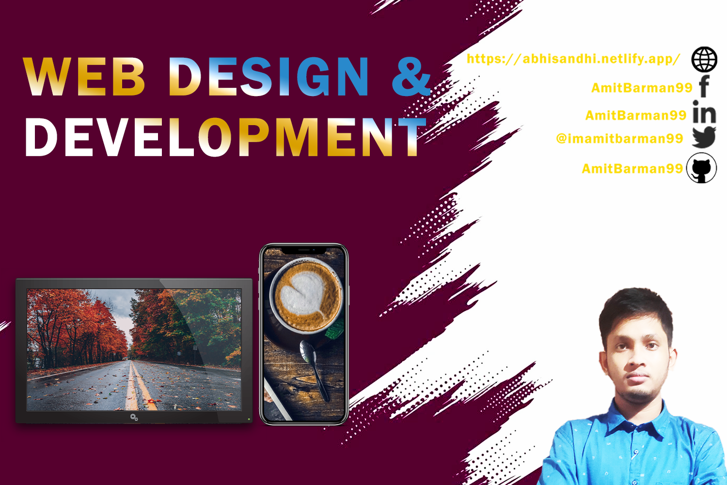
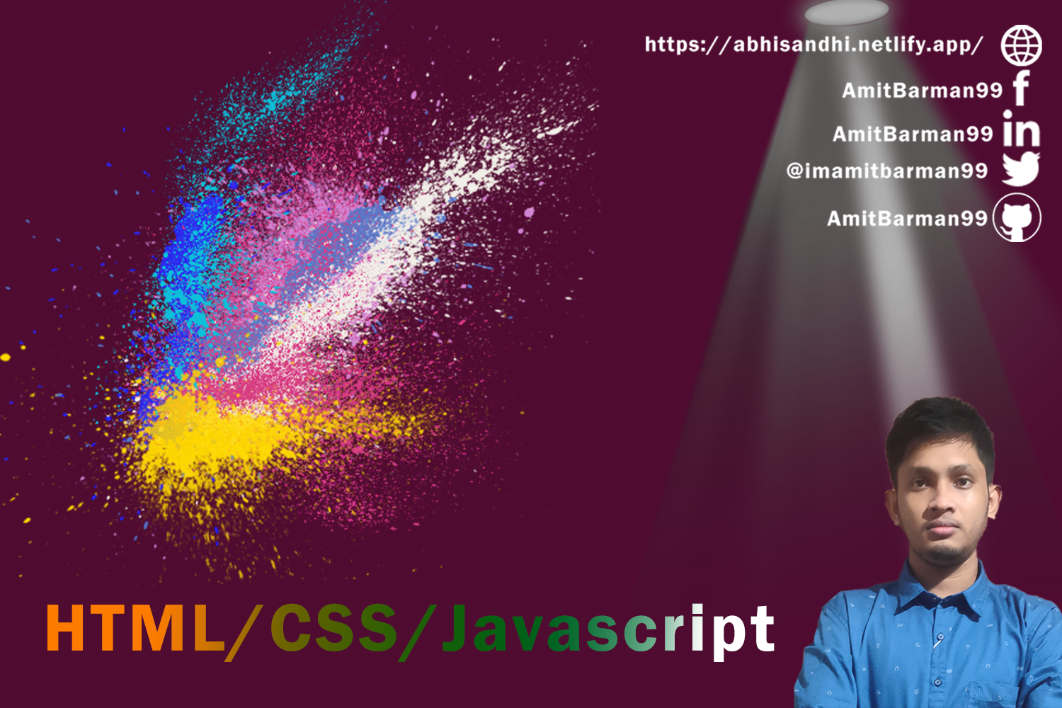
Here you can see all projects which is designed or developed or customized by me. I use VScode for HTML,CSS,javascript,C/C++, EasyEDA and kiCAD for circuit design and PCB designing, Electric for SSI layout design and LTSpice for simulation, Arduino for Arduino programming and Processing for Arduino-processing. For my Electronics related projects, please switch to my Engineering profile..
Click here to see my all project's images in box-design.
Click here to see my all html project's images .
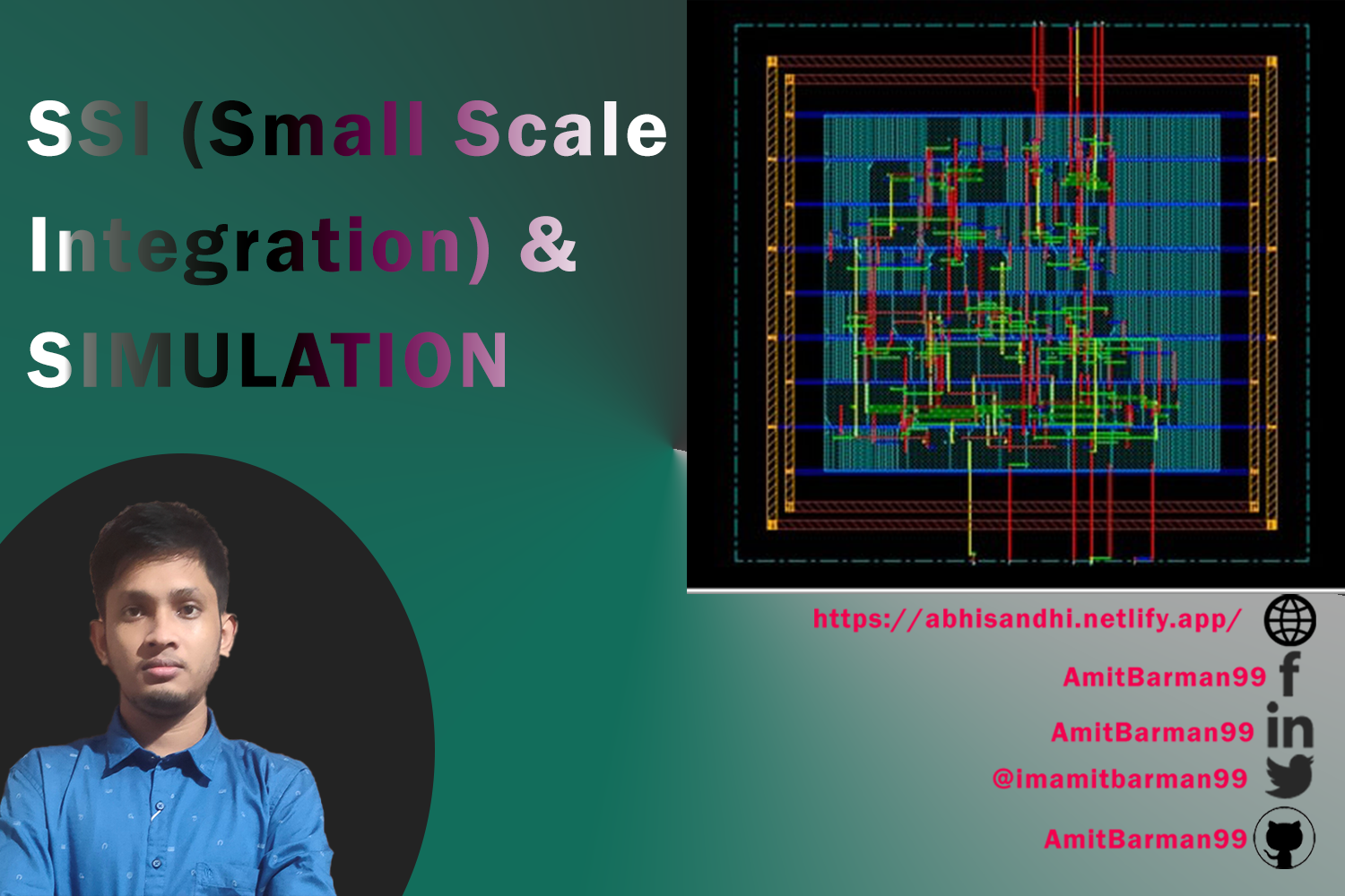
Click here to see my only SSI layout and simulation project's images.
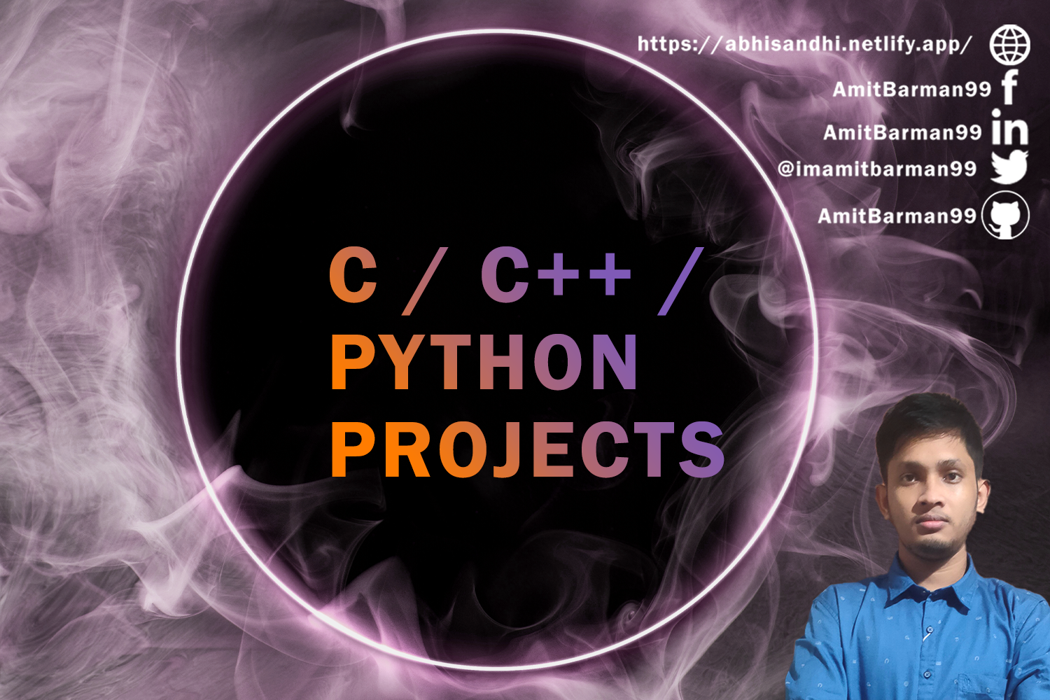
Click here to see my all python / C / C++ project's images.
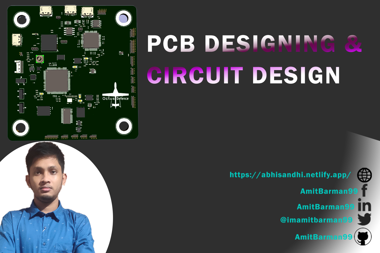
Click here to see my all circuit and PCB design project's images.
Click here to see my all other type project's images.
Here is my Timeline of my improvement of developing skills.
Space electronics , rover, probe technology, Semiconductor devices payloads etc.
Aircraft's electronics warfare system, radar system and all other hardware parts.

VLSI technology, SemT Devices, UAV electronics, 6th gen. Aircrafts technology, ASIC, RF device/ MMIC.
VLSI chip designing, Quantum devices & Sensors, Space telescope, Rover, Probe related things.
Space electronics , rover, probe technology, Semiconductor devices payloads etc.
Aircraft's electronics warfare system, radar system and all other hardware parts.
VLSI technology, SemT Devices, UAV electronics, 6th gen. Aircrafts technology, ASIC, RF device/ MMIC.
VLSI chip designing, Quantum devices & Sensors, Space telescope, Rover, Probe related things.
I am working on improving my Resume. So, during update time I am trying to improve best from my side. You will find all about my Resume.
Thanking you,
You can contact me from here also. You can sent me mail with your projects and also call me from 10am to 7pm in a day. Enjoy this websites...